

Hey so today we are going to be doing something different. We are moving from the field of embedded systems to the field of VLSI. I have always been interested in VLSI (Very Large-Scale Integration) but projects in the field are not easy to experiment. It is not too hard to develop a project in embedded systems but there is no satisfying project you can do in the field in VLSI. However, today I’m going to be trying a VLSI based project. I’m going to be reverse engineering a die shot of an IC.
Basics
For those who are from a less technical background I’ll give you a brief introduction about what I mean. An IC is an integrated circuit. It basically is a regular circuit which is implemented in a very small area. Everything is implemented in the form of transistors and resistors. For example, a AND gate is just a combination of transistors. So, everything in electronics is made from transistors. A die is basically the building block on to which the transistors are printed on. (They aren’t actually printed, it more like spray paint with masks and etching using photolithography) The die is the silicon on which the circuit is implemented. This circuit is then placed in a plastic enclosure and packed as an IC.
Plan
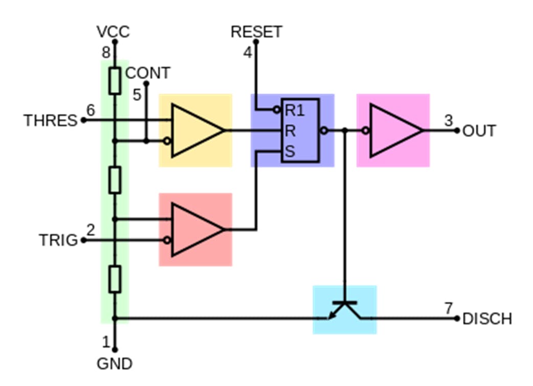
What I want to do is find out the functionality of a chip from the die image and identify each transistor. Actually, I already kind of did it in a YouTube video which is a screen recording of me in m.s. paint which you can watch here but I assumed a blog would be more efficient.The IC I choose is the 555 timer IC. It is very popular and a lot of you probably used it at some point. It is a timing IC which will give you a clock signal whose duty cycle can be varied. If you want to learn the working of the 555 I suggest this video by Ben Eater and if you want to see my previous project with the 555 you can find it here. The reason I choose the 555 is because it is very popular so there is a lot of documentation on it and also because it is a relatively simple IC without many transistors, making it a good place to start.
Decapping the IC
So first we need to take a 555 timer IC. It is very popular to find it in a DIP package, you can buy one here. The next thing we need to do is remove the metal contacts and the plastic coating. This is done with concentrated sulfuric and nitric acids. You can see the process Here Once the die is visible we can clean it and take pictures of it under a microscope. Normally many pictures are taken and then stitched together in software to get a clear high-definition image. Now we have our die image. As you can imagine, I don’t have the expertise to do this process. Luckily for me there are a lot of nice people who did this process and upload their images for free. One such person is Richi. He has a blog where he has documented many different IC. I would urge you to check out his site, Richi’s Lab and support him. Without him, my project will not be possible. He has documented every major 555 Timer IC available and uploaded die images here he has included both bipolar and CMOS technology. I am going to go with the Fairchild uA555 as my choice of IC. There not much behind this decision, you can go with any of the manufactures, each one with a different configuration. I would say that CMOS are harder to get a hold of that Bipolar types.
References
Before I go on let me show you what I want to do. I just want to get as much information from the die as possible, I don’t expect to get all the information but if you want to see more professional reverse engineering then I would suggest the following:
Ken Shirriff`s blog
Ken Shirriff is one of my idols. I first saw his work when working with the Arduino, I used his IR remote library. Then I saw a talk he gave in the hacker day convention talking about reverse engineering IC, which you can watch here.This led me to his blog which you should check out. He has reversed engineered a 555 timer and made an interface where you can click on the schematic and the corresponding region on the die is highlighted or vice versa. This blog is what I wanted to implement. But at the same time even though my work is similar, I have made sure to figure out stuff on my own and not abuse his work.
YouTube
If you like reverse engineering IC then I suggest the following videos which I found very interesting. Another Ken Shirriff talk, A tutorial, a complex 6502, Robert Baruch, a short explanation and a live stream
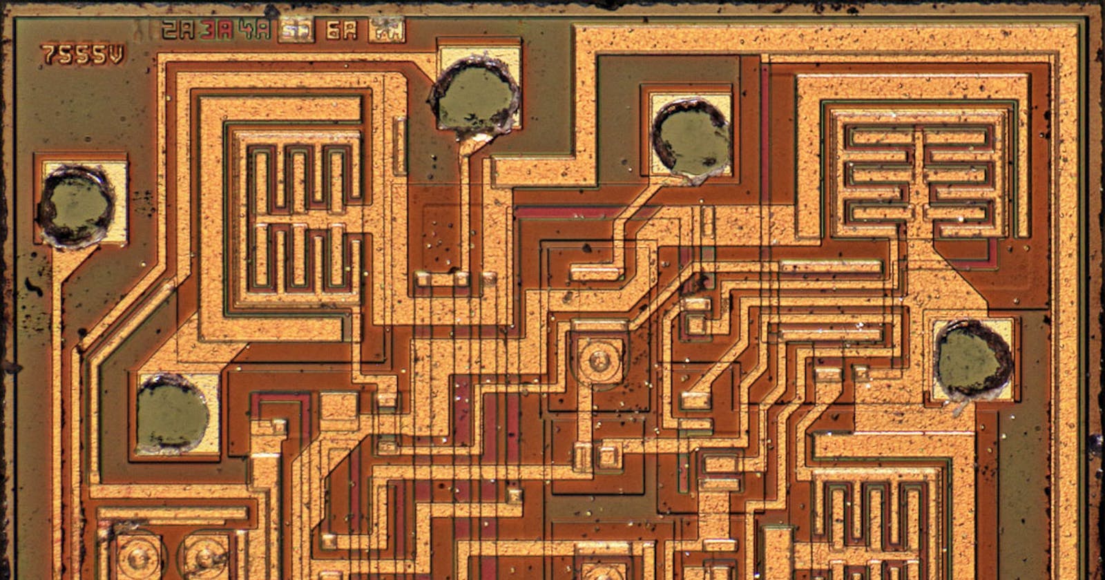
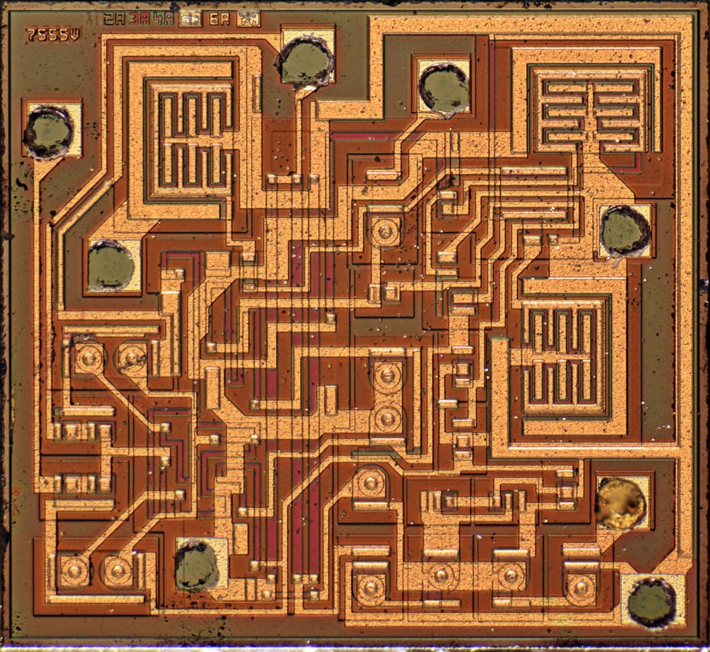
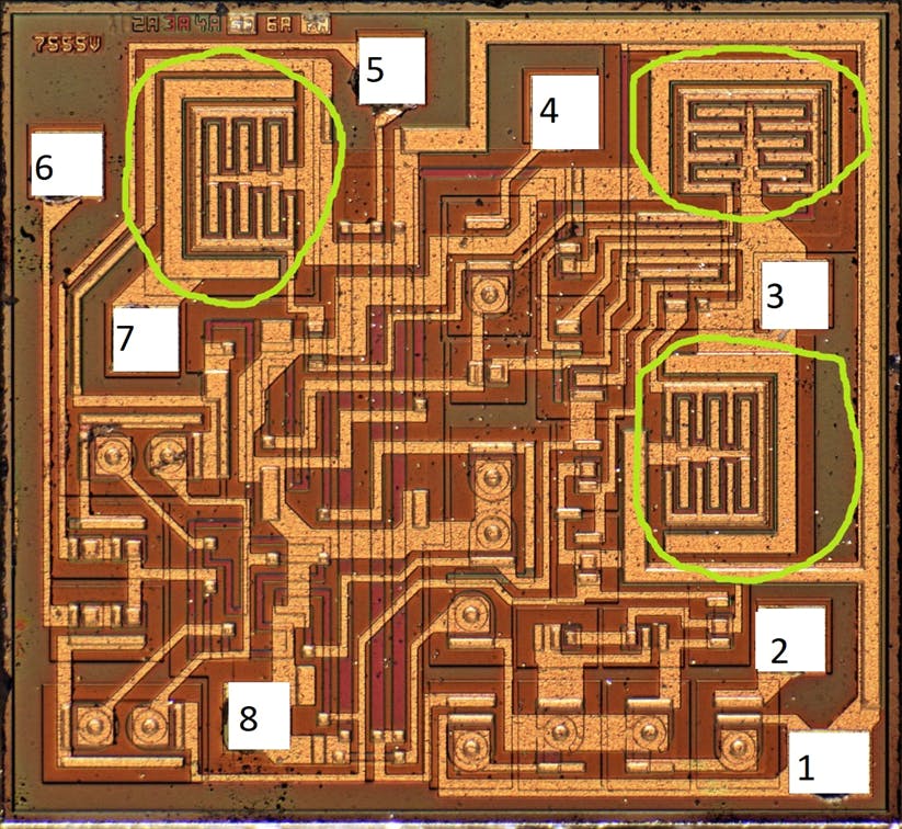
Die image
Pads
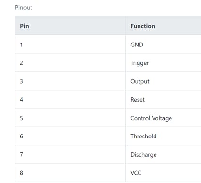
Now back to the project. The first thing we notice is the bond wires which connect the metal contacts of the IC to the pads on the die. These are just metal wires. Now we can identify the pads, there are 8 of them, each corresponding to a pin on the IC. We should try and figure out which pin is which. I like to find ground first, this is normally the pad which is connected to most of the circuit. Ground is normally required at many points in the circuit and so tends to go around the border of the circuit. This looks like the pad on the bottom right. I’m going to go with this as ground. Looking for a datasheet for the uA555 I was able to find a pin out as follows:
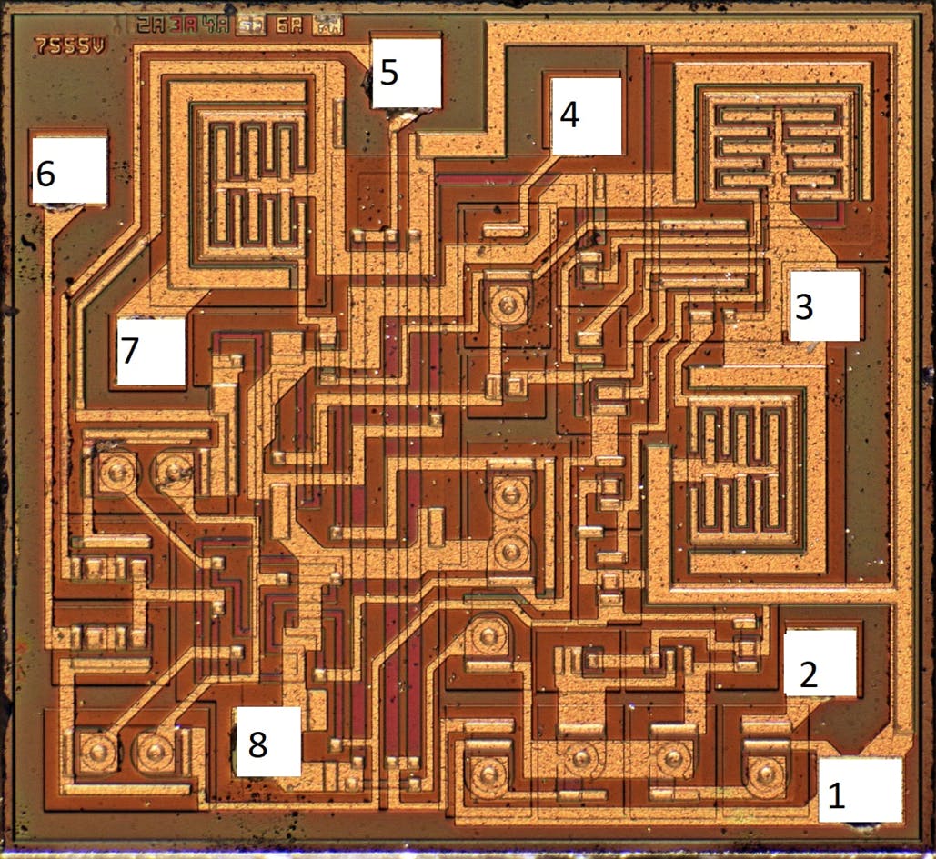
So, using this we can go in clockwise direction (or anticlockwise) direction and number all the pads like I did bellow:
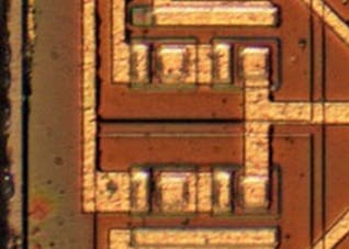
Now after numbering the pads, we need to go and identify transistors. For this we just need to see what significant pattern can we find on the die. I have marked 3 significant repeating patterns which I think are transistors bellow:
These are high current transistors, which means they are regular transistors which can produce a high current. Transistors are very simple devices, you can think of it as a switch, with 3 terminals the collector, emitter and base. The base can be thought of the actually switching part of the switch. When we turn the base on (by providing some voltage on it) the transistor turns on and current flows from the collector to the emitter (this is the case of NMOS, for PMOS it is opposite) In this high powered transistor the regions are as follows: The green is the collector, the red is the base and the orange is the emitter.
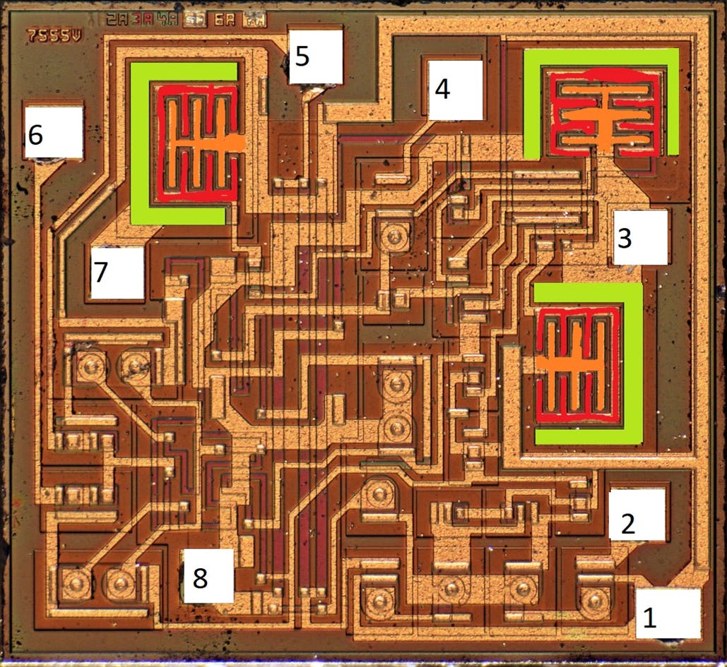
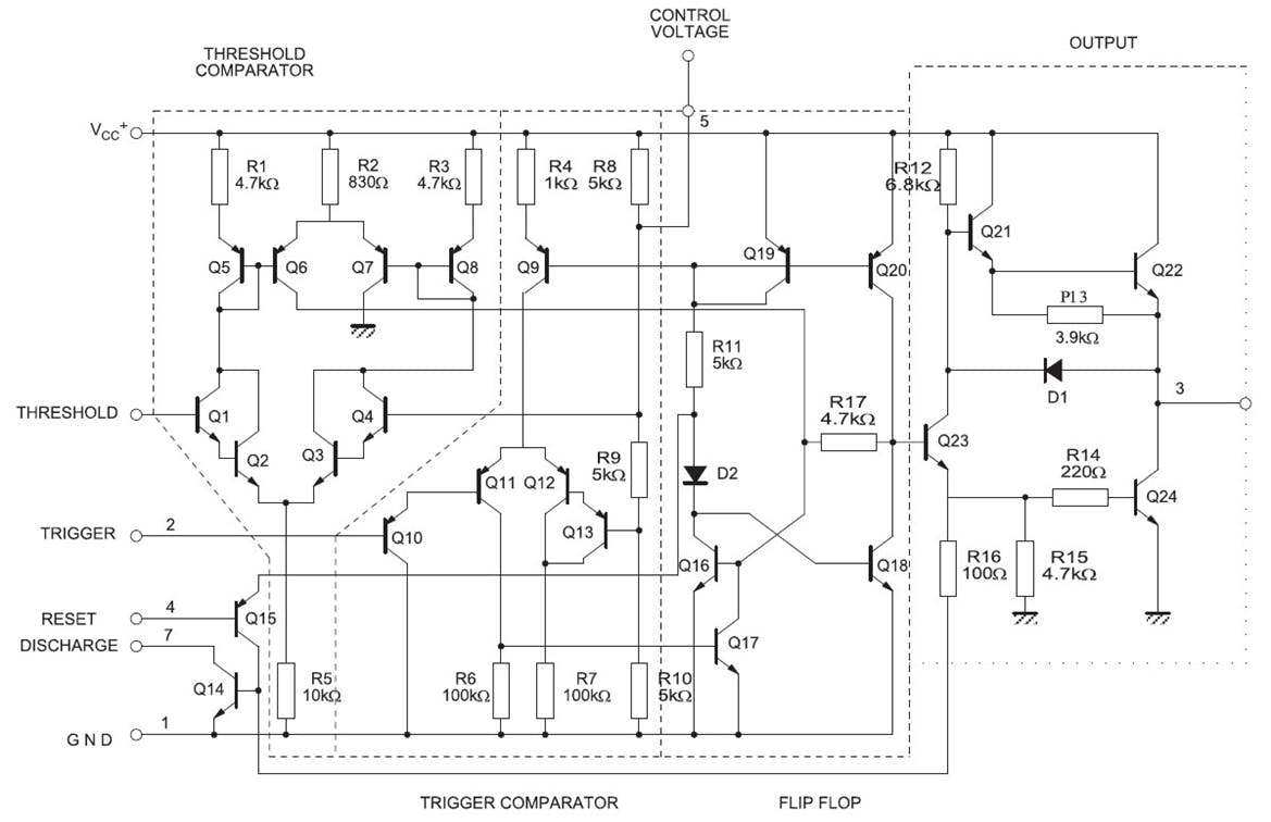
Great so now we have identified 3 transistors but we don’t know what they do, so let’s take a look at a schematic.

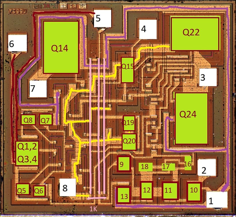
We can see that in our die image the emitter of the transistor on the top right is connected to pin 3 which is also connected to the collector of the other transistor. So that means pin 3, which corresponds to the output pin, is connected to 2 transistors. If we look at the schematic the output pins in connected to transistors Q22 and Q24. So, we have identified these two transistors. If we follow this process, we can see that the other transistor is connected to pin 7 which is the discharge pin, meaning that the transistor is Q14. We now identified the 3 main transistors.
Resistors
Now if we look at the block diagram of the 555, we can see that there is three 5Kohm resistors present.
Let us find this. In the die, a resistor is not very easy to identify, but if you look closely, you can see 3 straight lines through the middle. These are the resistors as I have drawn them out bellow:
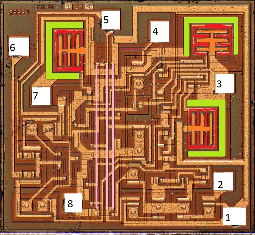
If you look at the ends of the resistors you can see that the left most resistor is connected to VCC (pin 8) and the other end of that resistor is connected to the end of the other resistor which is then connected to the third resistor. Whose end is connected to ground (Ill tell you why that’s ground latter) This shows us that the 3 resistors are connected in series, which is what we wanted to see.
Ground and VCC
Now let’s follow the path and mark out GND and VCC. I’ll use purple from ground and yellow for VCC.
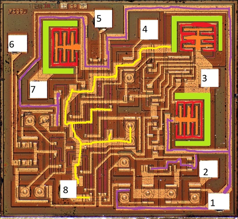
We can confirm a lot of our assumptions now, Firstly, one of the ends of the 5K resistor is connected to VCC and the other end of the last resistor is connected to ground. Secondly, according to the schematic the collector of Q22 is connected to VCC and the emitter of Q24 is connected to ground.
Transistors
Let’s now have a look at pad 6 which is the threshold pin, if we follow the line it seems to go to what we can call a npn transistor. We actually see 4 in a row, if we keep going, we reach pin 5 which is the control pin, if we look at the schematic pin 5 and pin 6 do seem to be connected so we are on the right path. If we follow pin 5 it also seems to be connected to the two 5k ohm resistors which is the case. So we can say that those 4 transistor were Q1,Q2,Q3,Q4.
I went along an identified Q9, Q10, Q11, Q12, Q13, A16, Q17 AND Q 18. I also identified the 1k ohm resistor R4. I then identified the rest of the transistors except Q21 and Q23. There are also some extra transistors which I haven’t marked those can be diodes or resistors as both diodes and resistors are implemented as transistors at times.
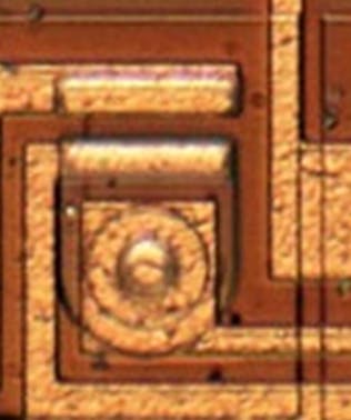
All I needed to identify was the difference between pnp and npn transistors. The arrow going in are pnp and are much bigger and circular in shape while the npn (arrow going out) are smaller and much harder to identify.
PNP transistor:
NPN transistor:
I think that all for the blog, if you want to know more watch the YouTube video bellow: