DIP Switch
Interfacing 7 way DP switch with Altera Cyclone II EP2C5

Hi, this blog is a way to keep all my projects in one place, while documenting the process along with all the problems that I encounter.
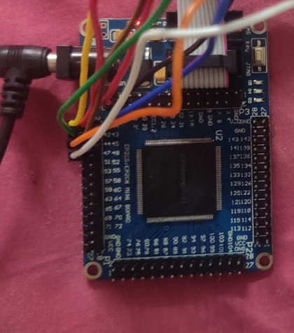
Hi, I been super excited to start working with my FPGA, the Altera Cyclone II EP2C5. A very common projects I see being implemented on FPGAs is controlling a 7-segment display with a DIP switch. Now I am just a beginner in Verilog coding so I thought I start a little smaller and implement an encoder. In this project I will connect up an 8-way DIP switch to the FPGA, and depending on the switch, I will display its equivalent binary on the onboard LED.
Hardware
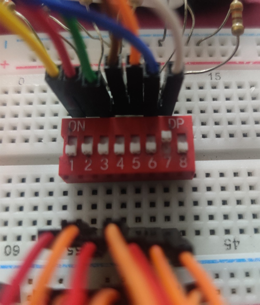
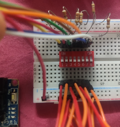
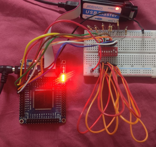
The first thing I needed was to connect up my DIP switch, you can find one at Tomson Electronics To connect it I used a bread board, some Jumper wires and a few pull-down resistors (10Kohm). I connected one end of all the switches to the VCC pin of the board. I used male to male jumpers for this. I connected the other end of all the switches to Ground through the pull-down resistors. Finally, I connected the side of the switch connect to ground to the board. I used pins 40, 41, 42, 43, 44, 45, 47 for this.
Code
Now its time to write some Verilog code to implement our encoder.
module project1(a,b,c,d,e,f,g,led1,led2,led3);
input a;
input b;
input c;
input d;
input e;
input f;
input g;
output led1;
output led2;
output led3;

reg led1,led2,led3;
wire a,b,c,d,e,f,g;

supply0 x;
supply1 z;

always @(a,b,c,d,e,f,g)
case({g,f,e,d,c,b,a})
7'b0000001:
begin
led1=z;
led2=z;
led3=x;
end

7'b0000010:
begin
led1=z;
led2=x;
led3=z;
end

7'b0000100:
begin
led1=z;
led2=x;
led3=x;
end

7'b0001000:
begin
led1=x;
led2=z;
led3=z;
end

7'b0010000:
begin
led1=x;
led2=z;
led3=x;
end

7'b0100000:
begin
led1=x;
led2=x;
led3=z;
end

7'b1000000:
begin
led1=x;
led2=x;
led3=x;
end

default
begin
led1=z;
led2=z;
led3=z;
end

endcase
endmodule
The first line is our module declaration where we define our module and all the input and output signals. We then write the sensitivity list where the pins are either input or output. Finally, I declare the data types and the keywords to supply logic zero and logic one. One thing to note is that this board works with negative logic. That is to say the onboard led will work the opposite way to what you expect it to do. To fix this I use “x” for logic 0 instead of logic 1 and the same for “z”. The next part of the code is declaring the always block. In this block we need to define all the signals involved in this block. To make the code easier to write I use a case statement. In this case statement I use the concatenation operator, the curly brackets. This will do something to string concatenation in python if you are familiar. I define it from “g” to “a” as I want to use MSB first.
Finally, I write the output for each input case. It is important to write a default block as this works similar to an else statement. I use it to display nothing for invalid inputs. With that we can end the case and end the module.
Output
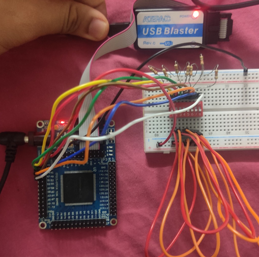
Now we can go ahead and program the board after compiling and assigning the pins. If you require any assistance in this part, please read my previous blog where I explain this in detail. I went ahead and powered up my board and connected the USB blaster and programmed the board.
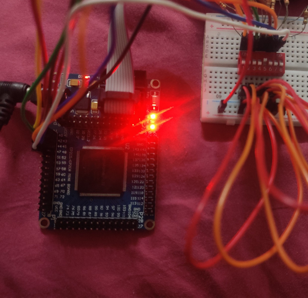 ^ for input 5: output = 101
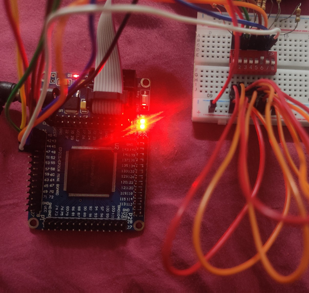 ^ for input 6: output = 110
 ^ for input 7: output = 111
In my next project I will be extending this project to display the data on a 7-segment display.


